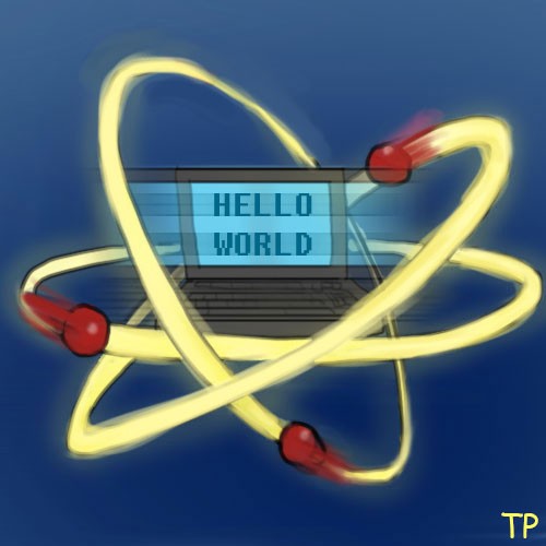
Nanotechnology: First computer processing unit made atom by atom. This being the first
"atomic" computer chip.
What this means is the further shrinking of the computer chip until its electrical lines (electrical wiring) are the width of one atom and separated from another electrical line by the width of an atom. An objection to this ultimate reduction is that electricity will jump from line to line and thus rendering such a chip useless. However, this is 2D thinking of chip construction. If instead, each electrical line is encased within non-conductive atoms (atoms which do not allow electricity to pass through them), this "bleed-over" problem is solved. Currently, computer chips are created by lithography. Lithography is essentially the using of a negative pattern to etch a pattern into something else. With current computer chips, the negative pattern is laid over a material, a burst of powerful short-wave radiation is flashed above the negative pattern, and this radiation burns the pattern into the material to create a computer chip. Making computer chips this way has essentially only "open air" between their electrical lines and this thus enables electricity to jump from one electrical line to the next if the lines are too close together.
However, if the electrical lines are encased in non-conductive material, the bleed-over won't then occur. But simply dipping such a chip into material to so coat it with non-conductive material doesn't solve the problem because each chip's billions of transistors would then be prevented from switching off and on. BUT nanotechnology solves this problem by construction of non-conductive encasements around the transistors that give them enough space to turn off and on. Essentially, what an atomic chip has is tunnels for its electrical lines and caverns for its transistors. And these non-conductive tunnels and caverns should enhance performance of the computer chip by only giving limited mobility to electricity sent through it. The electricity can only go down the electrical lines and doesn't have the option of leaving them. [By the way, technically, these are 3D computer chips because the encasements are not 2D structures but this challenge doesn't call them that. To Jack Decker (BTC's creator and the creator of this challenge), 3D computer chips (such as those mentioned in Future Challenges #18+) mean layer of electrical lines and transistors on top of each other.]
Future Challenges: 1) 8008
2) 8088
3) 386
4) Pentium
5) P4
6) z196
7) Xeon Phi 5110P
First atom-by-atom computer chip (which can outperform a Xeon Phi 5110P chip) made by a fully-automated system where 1,000 chips are made within:
8) 1,000 hours (~42 days)
9) 100 hours (~4 days)
10) 10 hours
11) 1 hour
12) 6 minutes
13) 36 seconds
14) 3.6 seconds
First atomic computer chip sold by private industry for:
15) Supercomputers
16) Desktop computers
17) Laptop computers.
18) Cellphones.
First atomic 3D wafer-level chip stacking to outperform a:
19) P4
20) z196
21) Xeon Phi 5110P
First atomic 3D chip (which can outperform a Xeon Phi 5110P chip) made by a fully-automated system where 1,000 chips are made within:
22) 1 hour.
23) 6 minutes.
24) 36 seconds.
25) 3.6 seconds.
First atomic 3D chip sold by private industry for:
26) Supercomputers.
27) Desktop computers.
28) Laptop computers
29) Cellphones